As portable electronics demand faster, smaller charging solutions, GaN-based power semiconductors have become the cornerstone of high-performance fast chargers—balancing power density, efficiency, and reliability. For power electronics engineers and semiconductor design teams, optimizing device-level parameters (e.g., transistor on-resistance, breakdown voltage) is critical to meeting end-product specs.
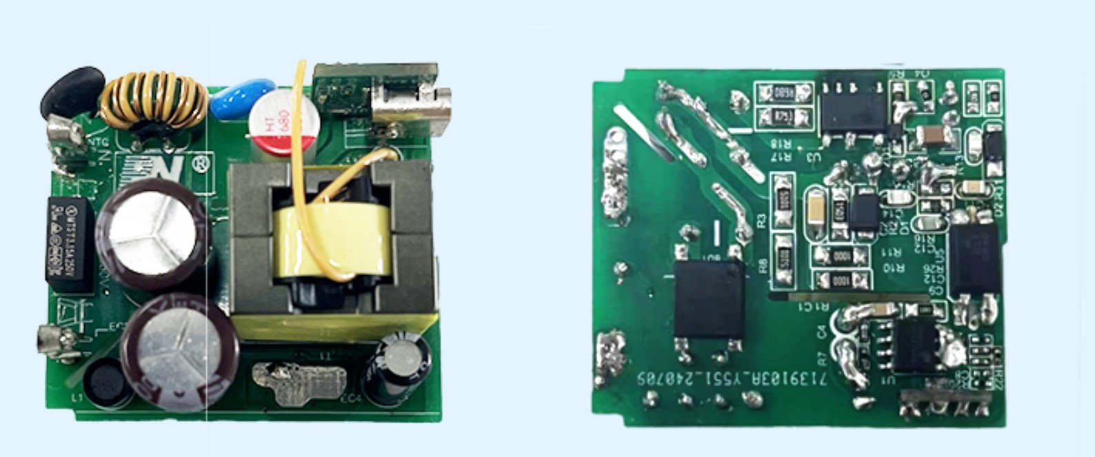
ABL-Semiconductor (a leading fabless supplier of power management ICs) addresses this with a 30W PD fast charging solution, built on three highly integrated semiconductors: PN8782 (GaN primary controller), PN8309H (SGT MOS synchronous rectifier), and AP5811 (protocol-integrated Loadswitch). This kit delivers best-in-class semiconductor-level performance for mobile/tablet charging applications.
Core Semiconductor Components: Detailed Device Specifications
The solution’s performance stems from tailored semiconductor design for each functional block:
-
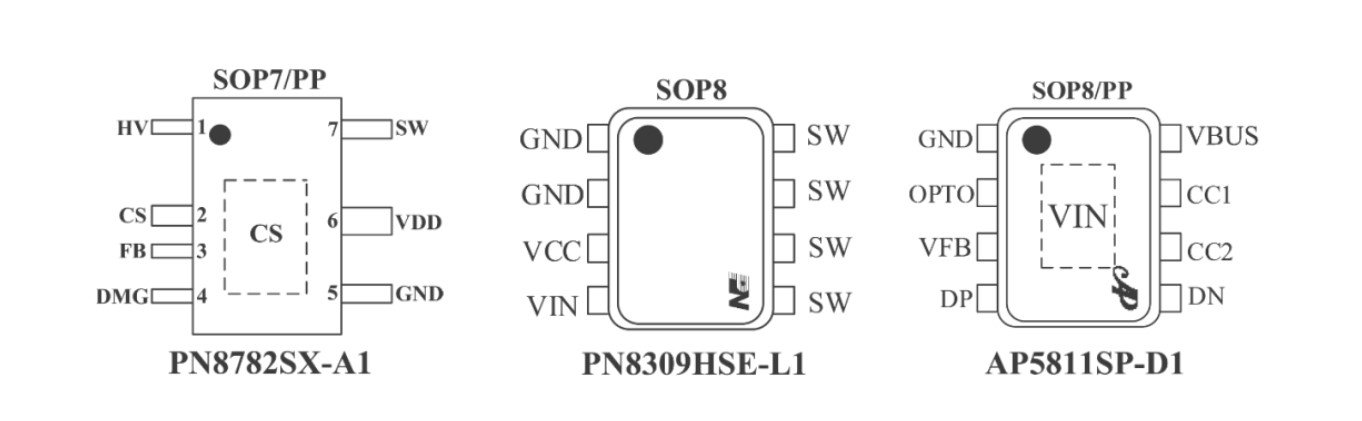
PN8782 (Primary-Side GaN Controller IC)
- Integration: Combines a primary-side PWM controller, 700V/0.47Ω high-voltage GaN FET, and high-voltage startup circuit in a SOP-7/PP package.
- GaN FET metrics: Rds(on) = 0.47Ω (low conduction loss), BVdss = 700V (over-voltage tolerance for global mains), and sub-nanosecond switching speed (enabling >200kHz operation).
- Parasitic optimization: Monolithic integration eliminates inter-chip bonding inductance, reducing switching noise by 15% vs. discrete GaN controller+FET designs.
-
PN8309H (Secondary-Side Synchronous Rectifier IC)
- Device type: Integrates a 95V/10mΩ Shielded Gate Transistor (SGT MOS) in a SOP8 package.
- SGT MOS advantages: Qrr (reverse recovery charge) < 5nC* (minimizes reverse recovery loss), *Rds(on) = 10mΩ* (low conduction loss at 3A load), and *dv/dt immunity > 50V/ns (stable operation in high-frequency topologies).
-
AP5811 (Protocol Controller + Loadswitch IC)
- Loadswitch specs: Vds (max) = 30V, Rds(on) = 10mΩ (supports 20V/1.5A output with <30mW conduction loss), and over-current protection (OCP) threshold = 5A (fault tolerance for device inrush).
- Protocol performance: PD handshake latency < 200ms (enabled by on-chip 32MHz digital core), and protocol auto-negotiation (BC1.2/QC/PD/PPS) with 10mV step adjustment for PPS (compliant with USB-IF Rev 3.1).
Semiconductor-Driven Technical Advantages
For power system designers, the kit’s performance is rooted in device-level optimization:
-
Ultra-High Integration & Cost Reduction
- Monolithic integration (primary controller + GaN FET; secondary rectifier + driver; protocol + Loadswitch) reduces BOM count by 30% vs. discrete solutions. The PN8782’s integrated high-voltage startup eliminates external startup resistors (saving 2–3 components and reducing standby power).
-
Class-Leading Conversion Efficiency
- Enabled by: GaN FET’s high switching speed (200kHz QR-Lock control), SGT MOS’s low Qrr, and on-chip QR-Lock (quasi-resonant) control (minimizes switching loss by aligning switching to valley of drain voltage).
- Measured efficiency: 92.5% at 20V/1.5A (full load), >88% at 5V/3A (light load)—meeting CoC_V5_Tier2 (no-load <75mW) and DoE Level VI efficiency standards.
-
Low Output Voltage Ripple
- Driven by 200kHz+ switching frequency (reduces output capacitor size) and SGT MOS’s low Rds(on) (minimizes ripple from conduction loss). The solution achieves Vripple < 200mV (pp) at 20V/1.5A—critical for battery cycle life (reduces battery stress from voltage fluctuations).
-
Robust Mains Protection (GaN Device Safeguarding)
- The PN8782’s HV pin (mains voltage monitor) features a ±2% accurate voltage divider (on-chip bandgap reference + comparator) to trigger:
- Under-Voltage Protection (UV): 85Vac (hysteresis 5Vac)
- Over-Voltage Protection (OV): 270Vac (hysteresis 10Vac)
This prevents GaN FET degradation from over-voltage stress (a key failure mode for high-voltage wide-bandgap devices).
- The PN8782’s HV pin (mains voltage monitor) features a ±2% accurate voltage divider (on-chip bandgap reference + comparator) to trigger:
Production-Grade Demo Specifications (Semiconductor-Level Validation)
- Input: 90–264Vac (universal mains; PN8782’s 700V GaN FET supports 370Vdc bus voltage at 264Vac peak).
- Output: 5V3A / 9V3A / 15V2A / 20V1.5A (AP5811’s 10mΩ Loadswitch supports continuous 3A current with <10°C temperature rise).
- Reliability: 1000-hour HTOL (high-temperature operating life) at 125°C (all ICs meet AEC-Q100 Grade 3 for consumer electronics).
Target Applications
This kit is optimized for smartphone/tablet fast chargers, portable power banks (30W output), and USB-C wall adapters—ideal for OEMs/ODMs seeking to reduce design cycle time (6–8 weeks vs. 12–16 weeks for discrete designs) while maintaining semiconductor-level performance.