
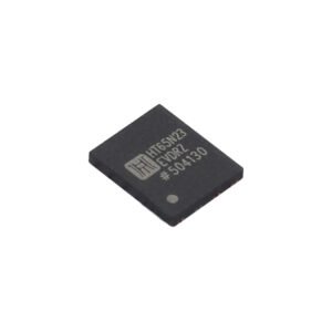
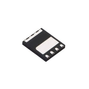
HT65N23E Overview
The HTCSEMI HT65N23E is a 650V enhancement-mode GaN-on-Silicon power transistor built for next-generation high-frequency, high-efficiency power conversion. Unlike depletion-mode GaN devices, the HT65N23E operates as a normally-OFF switch, making it a drop-in behavioural replacement for silicon MOSFETs in existing gate driver architectures without requiring additional circuit modifications for safe start-up. HTCSEMI’s GaN process delivers a maximum on-resistance of 140mΩ with a typical gate charge of just 3.3nC, resulting in extremely low switching losses and enabling power supply designs that achieve high efficiency at switching frequencies in the MHz range.
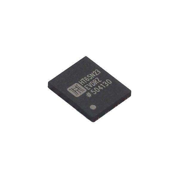
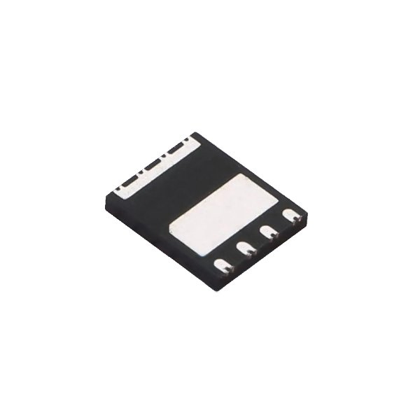
A standout characteristic of the HT65N23E is its zero reverse-recovery charge — a fundamental limitation of silicon body diodes that causes significant switching losses and EMI in hard-switched topologies. Combined with a low output charge (QOSS = 33nC at 400V) and ultra-fast switching transitions, the HT65N23E is particularly well-matched to totem-pole bridgeless PFC, LLC resonant half-bridge, and high-frequency DC-DC converter topologies. The device also incorporates integrated ESD safeguards, improving robustness during PCB assembly and field operation. The compact PDFN-8L (5mm × 6mm) dual flat no-lead package minimises parasitic inductance in the switching loop and supports high-density PCB layouts.
HTCSEMI positions the HT65N23E as a competitively priced alternative to established GaN FETs from GaN Systems, Infineon, and Transphorm. ABL Semi stocks the HT65N23E as a fully authentic, original factory product, providing engineers and procurement teams across the UK and Europe with a reliable, compliance-documented supply route, flexible MOQ, and multi-currency settlement options.
Key Specifications
| Parameter | Value |
|---|---|
| Device Type | 650V N-Channel Enhancement-Mode GaN-on-Silicon FET |
| Maximum Drain-Source Voltage (VDS,max) | 650V |
| Maximum On-Resistance (RDS(on),max) | 140mΩ |
| Typical Gate Charge (QG,typ) | 3.3nC |
| Pulsed Drain Current (ID,Pulse) | 32A |
| Output Charge at 400V (QOSS) | 33nC |
| Reverse Recovery Charge (Qrr) | Zero (GaN body diode characteristic) |
| Gate Drive Mode | Enhancement-mode (Normally-OFF) |
| ESD Protection | Integrated ESD safeguard |
| Package | PDFN-8L (5mm × 6mm) |
| Compliance | RoHS, Pb-free, REACH compliant |
Applications
The HT65N23E is designed for high-efficiency, high-frequency power conversion applications where silicon MOSFET switching performance is a limiting factor. Key application areas include totem-pole bridgeless PFC stages, LLC resonant converters, server and telecom power supplies, EV on-board chargers (OBC), and high-density DC-DC converters. The device is equally well-suited to solar microinverters, industrial SMPS designs, and motor drive systems demanding ultra-fast switching, minimal EMI, and compact PCB footprints enabled by GaN technology.
Pin-to-Pin Compatible Alternatives
The HT65N23E’s PDFN-8L (5×6mm) footprint and enhancement-mode gate interface are shared with leading Western-brand 650V GaN FETs, allowing direct substitution on existing PCB layouts to reduce BOM cost and broaden supply chain options without hardware redesign.
| Reference Part Number | Original Manufacturer | Why Choose HT65N23E |
|---|---|---|
| GS66502B | GaN Systems | Same 650V enhancement-mode GaN FET in a compatible DFN footprint; HT65N23E offers equivalent switching performance at a more competitive unit price from ABL Semi stock |
| EPC2054 | Efficient Power Conversion (EPC) | Comparable low-QG GaN FET targeting high-frequency applications; HT65N23E provides a higher 32A pulsed current rating with integrated ESD protection |
| TP65H150G4LSQA | Transphorm | 650V GaN FET in a similar surface-mount package; HT65N23E delivers lower gate charge (3.3nC) for reduced gate drive losses at high switching frequencies |
| IGT40R070D1 | Infineon (CoolGaN) | Infineon’s 650V enhancement-mode GaN transistor in comparable DFN package; HT65N23E provides a cost-effective domestically sourced alternative with equivalent normally-OFF operation |
Frequently Asked Questions
Is HT65N23E RoHS compliant?
Yes. The HT65N23E is fully RoHS, Pb-free, and REACH compliant. HTCSEMI manufactures the HT65N23E in accordance with EU RoHS Directive 2011/65/EU, ensuring the device is free from restricted hazardous substances. ABL Semi can supply full compliance and trade documentation upon request to support UK and European regulatory requirements.
What are the pin-to-pin replacements for HT65N23E?
The HT65N23E is a direct footprint-compatible alternative to several leading 650V enhancement-mode GaN FETs, including the GaN Systems GS66502B, EPC EPC2054, Transphorm TP65H150G4LSQA, and Infineon IGT40R070D1, all sharing a comparable DFN/PDFN (5×6mm) package and normally-OFF gate drive interface. Please refer to the compatibility table above for a detailed technical comparison.
What is the minimum order quantity (MOQ) for HT65N23E?
ABL Semi offers flexible MOQ for HT65N23E, supporting both prototype quantities and mass production orders. Contact us for current stock and pricing.
What package options are available for HT65N23E?
The HT65N23E is available in the PDFN-8L (5mm × 6mm) package — a compact dual flat no-lead SMD format that minimises switching loop inductance, a critical factor in achieving clean, low-loss waveforms in high-frequency GaN-based converter designs. This package is footprint-compatible with industry-standard DFN (5×6mm) GaN FET housings used by multiple leading suppliers. Contact ABL Semi to confirm current stock availability.
What gate drive voltage is recommended for the HT65N23E?
As an enhancement-mode (normally-OFF) GaN FET, the HT65N23E is driven similarly to a conventional silicon MOSFET. A positive gate-source turn-on voltage (VGS) of +5V to +6V is typical for full enhancement and minimum RDS(on), while a turn-off voltage of 0V is generally sufficient — though a small negative bias of -3V may be applied in noise-sensitive high dV/dt environments to prevent spurious turn-on. Gate drive voltages must remain within the device’s rated VGS limits; standard GaN-compatible gate driver ICs with adequate peak current capability are recommended to fully exploit the HT65N23E’s fast switching characteristics.
For complete product specifications, please refer to: