
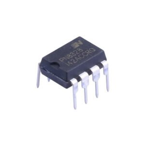
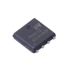
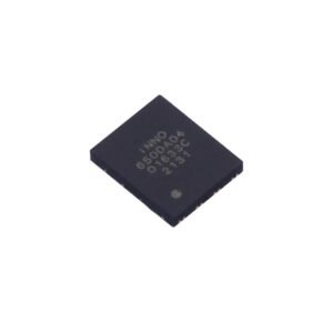
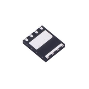
INN650DA04 Overview
The Innoscience INN650DA04 is a 650V enhancement-mode GaN-on-Silicon power transistor designed to push the boundaries of switching frequency and power density in modern converter topologies. Built on Innoscience’s proprietary GaN process, the INN650DA04 operates as a normally-OFF (enhancement-mode) switch, offering direct compatibility with standard silicon MOSFET gate driver circuits and eliminating the safety concerns associated with depletion-mode GaN devices. With a maximum RDS(on) of 480mΩ and a remarkably low typical gate charge of 0.9nC, the INN650DA04 is optimised for high-frequency topologies where minimising gate drive losses is as important as reducing conduction losses.
A defining characteristic of the INN650DA04 is its zero reverse-recovery charge — a property inherent to GaN transistors that eliminates the body diode recovery losses which limit silicon MOSFETs in hard-switched and semi-resonant topologies. The low output charge (QOSS = 8nC at 400V) further reduces switching transition losses, making the INN650DA04 particularly effective in totem-pole PFC, LLC resonant converters, and high-frequency DC-DC stages. Integrated ESD safeguards enhance device robustness during handling and assembly, and the INN650DA04 is qualified for industrial applications in accordance with JEDEC reliability standards — a key differentiator for engineers targeting industrial-grade system certifications.
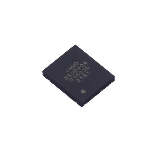
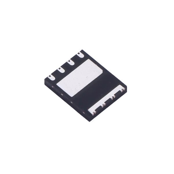
Housed in a compact DFN-8 (5mm × 6mm) dual flat no-lead package, the INN650DA04 minimises switching loop parasitic inductance and supports high-density PCB layouts. Innoscience is one of China’s leading dedicated GaN power semiconductor manufacturers, and the INN650DA04 represents a cost-competitive, performance-equivalent alternative to established GaN FETs from GaN Systems, EPC, and Transphorm. ABL Semi distributes the INN650DA04 as a fully authentic, original Innoscience factory product, with compliance documentation and flexible ordering to support UK and European design programmes.
Key Specifications
| Parameter | Value |
|---|---|
| Device Type | 650V N-Channel Enhancement-Mode GaN-on-Silicon FET |
| Maximum Drain-Source Voltage (VDS,max) | 650V |
| Maximum On-Resistance (RDS(on),max) | 480mΩ |
| Typical Gate Charge (QG,typ) | 0.9nC |
| Pulsed Drain-Source Current (IDS,Pulse) | 11A |
| Output Charge at 400V (QOSS) | 8nC |
| Reverse Recovery Charge (Qrr) | Zero (GaN characteristic) |
| Gate Drive Mode | Enhancement-mode (Normally-OFF) |
| Industrial Qualification | JEDEC standards qualified |
| ESD Protection | Integrated ESD safeguard |
| Package | DFN-8 (5mm × 6mm) |
| Compliance | RoHS, Pb-free, REACH compliant |
Applications
The INN650DA04 is suited to high-frequency, high-efficiency power conversion applications where GaN’s superior switching characteristics deliver measurable system-level benefits over silicon. Primary application areas include totem-pole bridgeless PFC stages, LLC resonant converters, high-density DC-DC converters, industrial SMPS, and server power supplies. The device is also well-matched to solar microinverters, EV auxiliary power modules, and consumer fast-charger adapter designs, where its ultra-low gate charge and zero reverse-recovery charge enable compact, efficient solutions compliant with modern energy efficiency standards.
Pin-to-Pin Compatible Alternatives
The INN650DA04’s industry-standard DFN-8 (5×6mm) footprint and enhancement-mode interface are shared across leading Western GaN FET suppliers, enabling direct board-level substitution to improve cost efficiency and supply chain resilience without any PCB layout changes.
| Reference Part Number | Original Manufacturer | Why Choose INN650DA04 |
|---|---|---|
| GS66502B | GaN Systems | 650V enhancement-mode GaN FET in a compatible DFN (5×6mm) footprint; INN650DA04 offers an equivalent zero-Qrr performance profile at a more competitive price point from ABL Semi stock |
| EPC2054 | Efficient Power Conversion (EPC) | Comparable low-gate-charge GaN transistor; INN650DA04 provides JEDEC industrial qualification and integrated ESD protection for greater design confidence in certified end products |
| TP65H600G4BS | Transphorm | 650V GaN FET in a similar surface-mount package; INN650DA04 delivers a lower QG of 0.9nC for reduced gate drive power at very high switching frequencies |
| IGT60R190D1 | Infineon (CoolGaN) | Infineon 650V enhancement-mode GaN in DFN format; INN650DA04 offers a domestically sourced, cost-optimised alternative with equivalent normally-OFF operation and JEDEC-level reliability qualification |
Frequently Asked Questions
Is INN650DA04 RoHS compliant?
Yes. The INN650DA04 is fully RoHS, Pb-free, and REACH compliant. Innoscience manufactures the INN650DA04 in accordance with EU RoHS Directive 2011/65/EU, ensuring the device is free from restricted hazardous substances including lead and mercury. ABL Semi can supply full compliance and trade documentation upon request to support UK and European regulatory and procurement requirements.
What are the pin-to-pin replacements for INN650DA04?
The INN650DA04 is a direct footprint-compatible replacement for several leading 650V enhancement-mode GaN FETs in the DFN-8 (5×6mm) package, including the GaN Systems GS66502B, EPC EPC2054, Transphorm TP65H600G4BS, and Innfineon IGT60R190D1. Refer to the compatibility table above for a full technical comparison of each alternative.
What is the minimum order quantity (MOQ) for INN650DA04?
ABL Semi offers flexible MOQ for INN650DA04, supporting both prototype quantities and mass production orders. Contact us for current stock and pricing.
What package options are available for INN650DA04?
The INN650DA04 is available in the DFN-8 (5mm × 6mm) dual flat no-lead SMD package. This compact footprint is the industry-standard housing for 650V GaN FETs across multiple suppliers, making it straightforward to adopt the INN650DA04 as a direct board-level replacement on existing PCB layouts. The low-inductance DFN package is particularly well-suited to high-frequency switching applications where parasitic loop inductance would otherwise degrade switching waveform quality. Contact ABL Semi to confirm current stock availability.
What gate drive voltage is recommended for the INN650DA04?
As an enhancement-mode (normally-OFF) GaN transistor, the INN650DA04 is compatible with standard silicon MOSFET gate driver ICs. A positive turn-on voltage of +5V to +6V is typically recommended to fully enhance the channel and achieve the rated minimum RDS(on), while a turn-off voltage of 0V is generally sufficient under normal operating conditions. In high dV/dt environments — common in totem-pole PFC and resonant half-bridge topologies — a small negative bias of -3V during turn-off may be applied to guard against cross-conduction from capacitive coupling. Given the INN650DA04’s ultra-low QG of 0.9nC, even modest peak gate drive currents are sufficient to achieve fast, clean switching transitions.
For complete product specifications, please refer to: