
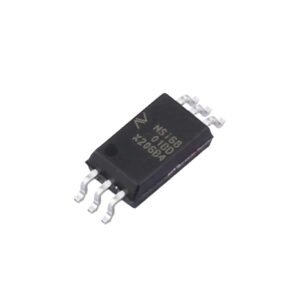
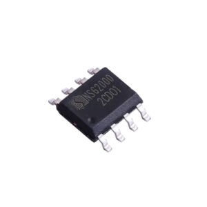


UTC 2SK3666 Overview
The UTC 2SK3666 is an N-channel junction silicon Field-Effect Transistor (JFET) manufactured using UTC’s advanced semiconductor process, delivering low IGSS (gate-source leakage current) and low CRSS (reverse transfer capacitance) in a compact SOT-23 package. As a depletion-mode JFET, the 2SK3666 conducts at zero gate bias and is controlled by applying a negative gate-source voltage to reduce drain current toward pinch-off — a characteristic that makes it inherently suited to analogue amplifier biasing circuits where a simple resistive gate bias is sufficient to set the operating point without complex enhancement-mode drive circuitry. The combination of low leakage and low capacitance results in excellent high-impedance signal handling and low noise performance at the low frequencies targeted by this device.
UTC has optimised the 2SK3666 for signal-level analogue applications rather than power switching, with key parameters including a VGS(off) of 950mV — a low and well-defined pinch-off voltage that simplifies biasing design in battery-powered circuits — an IDSS of 6mA establishing the maximum channel current at zero gate bias, and an RDS(on) of 270Ω, consistent with the high-impedance, small-signal character of JFET operation in this current range. Maximum power dissipation is 200mW, appropriate for the low-level signal conditioning roles the 2SK3666 addresses. Low CRSS is particularly valuable in high-impedance sensor interfaces, where input capacitance directly affects bandwidth and any capacitive feedback from drain to gate could cause oscillation or signal distortion at the frequencies of interest.
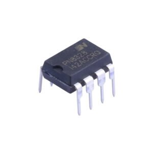
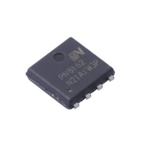
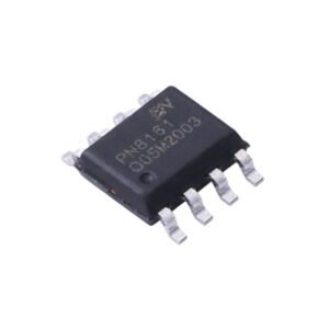
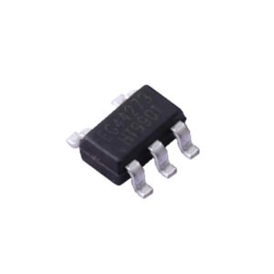
The UTC 2SK3666 is housed in the standard SOT-23 3-pin SMD package, universally used for small-signal discrete transistors and JFETs across consumer electronics and industrial sensing applications. UTC is a Taiwanese manufacturer with a long-established portfolio of analogue discrete devices, and the 2SK3666 is manufactured to full RoHS compliance. ABL Semi stocks the UTC 2SK3666 as a fully authentic, original factory product with flexible MOQ for both prototype and production quantities, and as a pin-to-pin alternative to equivalent N-channel JFETs from Toshiba, NXP, and Vishay in the same SOT-23 footprint.
Key Specifications
| Parameter | Value |
|---|---|
| Device Type | N-Channel Depletion-Mode Junction Silicon FET (JFET) |
| Saturation Drain Current (IDSS) | 6mA |
| Gate-Source Cutoff Voltage (VGS(off)) | 950mV |
| Drain-Source On-Resistance (RDS(on)) | 270Ω |
| Power Dissipation (PD) | 200mW |
| Gate Leakage Current (IGSS) | Low (UTC advanced process) |
| Reverse Transfer Capacitance (CRSS) | Low |
| Operating Mode | Depletion-mode (normally ON at VGS = 0) |
| Frequency Range | Low-frequency / general-purpose analogue |
| Package | SOT-23 |
| RoHS Compliance | Yes |
Applications
The UTC 2SK3666 is designed for low-frequency analogue signal processing applications where high input impedance, low leakage, and low noise are required in a compact, cost-effective discrete component. Primary application areas include infrared (IR) sensor preamplifiers, photodiode transimpedance amplifier input stages, general-purpose audio and low-frequency signal amplifiers, impedance buffer circuits, and analogue multiplexer switching stages. The device is equally applicable in environmental sensor conditioning circuits, precision instrumentation input stages, and low-power battery-operated sensing systems where the JFET’s depletion-mode operation, near-zero gate current, and low capacitance provide measurable performance advantages over bipolar transistors in high-impedance signal paths.
Pin-to-Pin Compatible Alternatives
The UTC 2SK3666’s SOT-23 package and N-channel JFET architecture are shared with equivalent small-signal JFETs from multiple established manufacturers, enabling direct board-level substitution to reduce BOM cost and establish alternative supply sources without any PCB layout changes.
| Reference Part Number | Original Manufacturer | Why Choose UTC 2SK3666 |
|---|---|---|
| 2SK3666 | Toshiba (original reference) | The original reference JFET this UTC device replaces; UTC 2SK3666 provides pin-identical SOT-23 substitution with equivalent low-IGSS and low-CRSS specification at a lower unit cost from ABL Semi |
| BF545B | NXP Semiconductors | N-channel JFET in SOT-23 for general-purpose amplification; UTC 2SK3666 provides a footprint-compatible alternative with comparable low-leakage characteristics suited to sensor and impedance converter applications |
| J111 | Vishay Siliconix | N-channel switching JFET in SOT-23; UTC 2SK3666 offers equivalent depletion-mode operation in the same package for low-frequency analogue and sensor signal conditioning at a competitive price |
| 2N5485 | Vishay / onsemi | N-channel JFET in SOT-23 for VHF and general-purpose use; UTC 2SK3666 provides a direct footprint replacement for low-frequency amplifier and sensor circuits with well-defined VGS(off) of 950mV |
| SST2N5484 | Microchip (Supertex) | Small-signal N-channel JFET in SOT-23; UTC 2SK3666 offers a pin-compatible alternative with low IGSS and low CRSS specifically optimised for impedance conversion and IR sensor front-ends |
Frequently Asked Questions
Is UTC 2SK3666 RoHS compliant?
Yes. The UTC 2SK3666 is fully RoHS compliant. UTC manufactures the 2SK3666 in accordance with EU RoHS Directive 2011/65/EU, ensuring the device is free from restricted hazardous substances including lead and mercury. ABL Semi can provide full compliance and trade documentation upon request to support UK and European regulatory and procurement requirements.
What are the pin-to-pin replacements for UTC 2SK3666?
The UTC 2SK3666 is a direct pin-to-pin replacement for the original Toshiba 2SK3666 and is footprint-compatible with equivalent N-channel JFETs in SOT-23, including the NXP BF545B, Vishay J111, Vishay/onsemi 2N5485, and Microchip SST2N5484. Refer to the compatibility table above for a detailed technical comparison.
What is the minimum order quantity (MOQ) for UTC 2SK3666?
ABL Semi offers flexible MOQ for UTC 2SK3666, supporting both prototype quantities and mass production orders. Contact us for current stock and pricing.
What package options are available for UTC 2SK3666?
The UTC 2SK3666 is available in the SOT-23 (3-pin small outline transistor) surface-mount package. This is the standard footprint for small-signal discrete JFETs across all major manufacturers, with the Gate–Source–Drain pin arrangement shared by equivalent devices from Toshiba, NXP, and Vishay — confirming the UTC 2SK3666 as a genuine drop-in board-level replacement. Contact ABL Semi to confirm current stock availability.
How should the UTC 2SK3666 be biased for use as a general-purpose amplifier or impedance buffer?
The UTC 2SK3666 operates as a depletion-mode N-channel JFET, meaning it conducts at VGS = 0V and is gradually turned off as a negative gate-source voltage is applied toward VGS(off) = 950mV. The most common and simplest biasing method is self-bias (source degeneration bias): a resistor (RS) is placed in the source-to-ground path, and the gate is connected to ground through a high-value resistor (RG, typically 1MΩ to maintain high input impedance). The drain current through RS develops a positive source voltage, effectively creating a negative VGS that sets the operating point. For the 2SK3666 with IDSS = 6mA and VGS(off) = 950mV, a quiescent drain current of approximately ID = IDSS/4 ≈ 1.5mA is a typical starting point, requiring RS = VGS(off)/4 / ID ≈ 160Ω. This approach provides stable, temperature-compensated biasing with no additional supply voltages.
For complete product specifications, please refer to: