
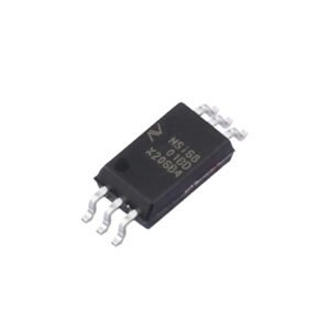
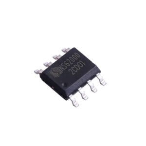


UTC 2SK508 Overview
The UTC 2SK508 is an N-channel depletion-mode Junction Field-Effect Transistor (JFET) optimised for high-frequency analogue amplification and RF signal processing in consumer and communications electronics. As a JFET device, the 2SK508 is a voltage-controlled current source that requires no gate drive current under DC bias conditions — making it ideal for high-impedance amplifier input stages where minimal loading of the source signal is essential. UTC has designed the 2SK508 with high forward transfer admittance (yfs/gm) and low input capacitance (Ciss), giving it excellent sensitivity and bandwidth in small-signal RF amplification roles — characteristics that directly determine gain and noise figure in tuner and radio front-end applications.
The UTC 2SK508 is specified with a gate-source cutoff voltage (VGS(off)) of 1.4V — a relatively low pinch-off voltage that allows operation from low supply voltages and simplifies biasing circuit design in battery-powered and portable equipment. The gate-source breakdown voltage (VGSS) is rated at 15V, providing adequate margin against electrostatic discharge and supply transients in typical receiver circuit environments. Maximum power dissipation is 200mW in the SOT-23 package, consistent with the low-signal, high-impedance nature of the applications the 2SK508 is designed for. As a depletion-mode N-channel JFET, the 2SK508 conducts at zero gate bias and is pinched off at a negative gate-source voltage — a fundamentally different operating mode from enhancement-mode MOSFETs, making it particularly suited to analogue amplifier and automatic gain control (AGC) circuit topologies.
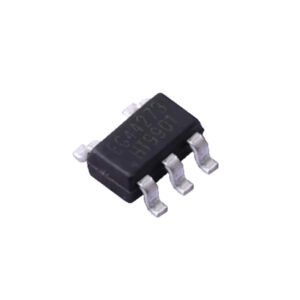
The UTC 2SK508 is housed in the industry-standard SOT-23 (3-pin small outline transistor) package — the most widely used SMD format for small-signal transistors and JFETs across the consumer and communications electronics industry. UTC is a Taiwanese semiconductor manufacturer with an extensive portfolio of discrete devices, and the 2SK508 is manufactured to full RoHS compliance. ABL Semi stocks the UTC 2SK508 as a fully authentic, original UTC factory product with flexible MOQ from prototype through to volume production, and pin-to-pin compatibility to established N-channel JFET equivalents from Toshiba, NXP, and VISHAY.
Key Specifications
| Parameter | Value |
|---|---|
| Device Type | N-Channel Depletion-Mode Junction FET (JFET) |
| Gate-Source Cutoff Voltage (VGS(off)) | 1.4V |
| Gate-Source Breakdown Voltage (VGSS) | 15V |
| Power Dissipation (PD) | 200mW |
| Key Characteristics | High forward transfer admittance (gm), low input capacitance |
| Operating Mode | Depletion-mode (normally ON at VGS = 0) |
| Gate Current | Near-zero (JFET — voltage-controlled) |
| Frequency Suitability | RF / HF (AM tuner, cordless telephone, wireless receiver front-ends) |
| Package | SOT-23 |
| RoHS Compliance | Yes |
Applications
The UTC 2SK508 is designed for small-signal, high-frequency amplification and switching applications in RF and analogue consumer electronics, where high transconductance, low input capacitance, and high input impedance are critical performance parameters. Primary application areas include cordless telephone RF receiver amplifiers, AM/FM tuner front-end stages, wireless LAN and short-range radio receiver inputs, analogue signal buffer amplifiers, and automatic gain control (AGC) circuits. The device is equally applicable in audio preamplifier input stages, low-noise sensor signal conditioning circuits, and oscillator circuits where the JFET’s near-zero gate current and low noise figure provide performance advantages over bipolar transistors in high-impedance signal path applications.
Pin-to-Pin Compatible Alternatives
The UTC 2SK508 is housed in the industry-standard SOT-23 package used universally for small-signal N-channel JFETs, enabling direct footprint substitution of widely deployed equivalents from Japanese and Western manufacturers to reduce BOM cost and diversify supply chain without PCB layout changes.
| Reference Part Number | Original Manufacturer | Why Choose UTC 2SK508 |
|---|---|---|
| 2SK508 | Toshiba (original) | The original reference JFET this UTC device is designed to replace; UTC 2SK508 provides pin-identical SOT-23 substitution with equivalent VGS(off) and high-gm characteristics at a lower unit cost |
| BF545A | NXP Semiconductors | N-channel JFET in SOT-23 for RF and amplifier applications; UTC 2SK508 provides comparable low-capacitance, high-transconductance performance with equivalent SOT-23 footprint compatibility |
| J112 | Vishay Siliconix | N-channel JFET in SOT-23 with similar pinch-off voltage range; UTC 2SK508 is a direct footprint replacement for AM tuner and wireless RF front-end applications at competitive pricing from ABL Semi |
| 2N5484 | Vishay / ON Semiconductor | Classic N-channel JFET for VHF/UHF amplifier use; UTC 2SK508 provides an equivalent low-noise, high-gm alternative in the same compact SOT-23 SMD format suitable for modern PCB designs |
| SST2N3819 | Microchip (Supertex) | N-channel JFET in SOT-23 for general-purpose and RF amplification; UTC 2SK508 offers comparable small-signal characteristics with a well-specified VGS(off) of 1.4V for consistent circuit bias design |
Frequently Asked Questions
Is UTC 2SK508 RoHS compliant?
Yes. The UTC 2SK508 is fully RoHS compliant. UTC manufactures the 2SK508 in accordance with EU RoHS Directive 2011/65/EU, ensuring the device is free from restricted hazardous substances including lead and mercury. ABL Semi can provide full compliance and trade documentation upon request to support UK and European regulatory and procurement requirements.
What are the pin-to-pin replacements for UTC 2SK508?
The UTC 2SK508 is a direct pin-to-pin replacement for the original Toshiba 2SK508 and is footprint-compatible with comparable N-channel JFETs in SOT-23, including the NXP BF545A, Vishay J112, Vishay/onsemi 2N5484, and Microchip SST2N3819. Refer to the compatibility table above for a detailed feature comparison.
What is the minimum order quantity (MOQ) for UTC 2SK508?
ABL Semi offers flexible MOQ for UTC 2SK508, supporting both prototype quantities and mass production orders. Contact us for current stock and pricing.
What package options are available for UTC 2SK508?
The UTC 2SK508 is available in the SOT-23 (3-pin small outline transistor) surface-mount package. SOT-23 is the industry-standard footprint for small-signal transistors and JFETs in SMD designs, with the Gate–Source–Drain pin arrangement shared across equivalent JFET devices from Toshiba, NXP, and Vishay — confirming the UTC 2SK508 as a direct board-level replacement. Contact ABL Semi to confirm current stock availability.
What is the difference between a JFET and a MOSFET, and why choose the UTC 2SK508 JFET for RF applications?
A JFET (Junction Field-Effect Transistor) and a MOSFET (Metal-Oxide-Semiconductor FET) are both voltage-controlled devices, but differ in their gate structure and operating characteristics. In a JFET such as the UTC 2SK508, the gate is a reverse-biased P-N junction — consuming effectively zero gate current under normal operating conditions and presenting an extremely high input impedance. This makes JFETs particularly advantageous in RF front-end and low-noise amplifier applications where: the source signal impedance is high; gate input capacitance must be minimised to preserve bandwidth; and low noise figure is critical. MOSFETs, while versatile, typically exhibit higher gate capacitance and can introduce more 1/f (flicker) noise at audio and lower RF frequencies. The UTC 2SK508’s combination of low VGS(off), high transconductance, and low Ciss makes it an optimised choice specifically for AM tuner, cordless telephone, and wireless receiver front-end circuits where these properties translate directly into improved signal sensitivity and selectivity.
For complete product specifications, please refer to: