
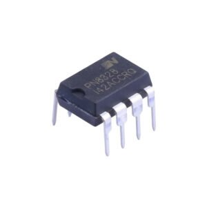
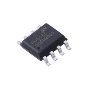
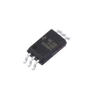
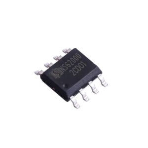
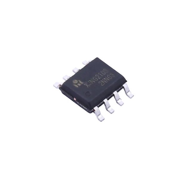
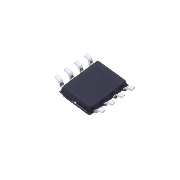
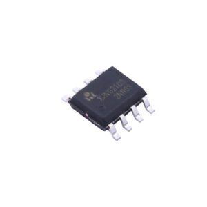
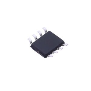
XJNG2103 Overview
The NCE XJNG2103 is a 200V high-voltage half-bridge gate driver IC featuring dependent high-side and low-side referenced output channels, designed to drive N-channel power MOSFETs in half-bridge, full-bridge, and synchronous buck converter power stages. Manufactured using proprietary HVIC and latch-immune CMOS process technology, the XJNG2103 achieves ruggedised monolithic construction that provides robust immunity against latch-up triggered by high dV/dt switching transients — a common failure mechanism in hard-switched power stages operating at high bus voltages. The floating high-side channel is designed for bootstrap operation and supports rail voltages fully up to +200V, making the XJNG2103 compatible with motor drive and inverter applications powered from rectified single-phase mains or high-voltage DC bus supplies.
NCE’s XJNG2103 delivers 1A symmetric peak source and sink output current on both channels, with a rise time of 50ns and a fall time of 40ns — providing fast, balanced gate switching transitions that minimise switching losses and reduce EMI in PWM-controlled half-bridge stages. The output drivers incorporate a high pulse current buffer stage designed for minimum cross-conduction, reducing the risk of simultaneous high-side and low-side conduction during fast switching transitions. The device operates from a gate drive supply of 9V to 20V and maintains a quiescent current of just 160µA, minimising self-heating and standby power draw in applications with variable load profiles. Input logic is fully compatible with 3.3V, standard CMOS, and LSTTL output levels, enabling direct interfacing to modern microcontrollers and DSPs.
The XJNG2103 floating channel is tolerant to negative transient voltages on the VS pin — a critical robustness characteristic in inductive load switching where VS can ring below ground during turn-off transitions without causing spurious device triggering or latch-up. The device is housed in the industry-standard SOIC-8 package, footprint-compatible with the widely deployed Infineon IR2103 and equivalent half-bridge driver ICs. ABL Semi stocks the XJNG2103 as a fully authentic, original NCE factory product, with flexible MOQ and compliance documentation for UK and European customers seeking a cost-effective, pin-to-pin alternative to established Western gate driver brands.
Key Specifications
| Parameter | Value |
|---|---|
| Device Type | Half-Bridge Gate Driver (High-Side + Low-Side) |
| Maximum Floating Channel Voltage | +200V |
| Gate Drive Supply Voltage | 9V to 20V |
| Peak Source Output Current (IOH) | 1A |
| Peak Sink Output Current (IOL) | 1A |
| Rise Time (TR) | 50ns |
| Fall Time (TF) | 40ns |
| Quiescent Current (Iq) | 160µA |
| Logic Input Compatibility | 3.3V, CMOS, LSTTL compatible |
| High-Side Supply Method | Bootstrap (floating channel) |
| Negative Transient Tolerance | Yes — dV/dt immune on VS pin |
| Technology | Proprietary HVIC + latch-immune CMOS |
| Package | SOIC-8 |
Applications
The XJNG2103 is well-suited to half-bridge and full-bridge power stage applications operating from high-voltage DC bus rails up to 200V, where a compact, robust gate driver with wide logic-level input compatibility is required. Primary application areas include BLDC motor drives, synchronous buck DC-DC converters, single-phase H-bridge inverters, solenoid and relay drivers, and class-D audio amplifier output stages. The device is equally applicable in e-bike and electric scooter motor controllers, industrial servo drives, and power tool variable-speed control stages, where its latch-immune HVIC construction, 160µA quiescent current, and SOIC-8 footprint provide a reliable and cost-efficient gate drive solution.
Pin-to-Pin Compatible Alternatives
The XJNG2103’s SOIC-8 package and dependent dual-channel half-bridge architecture are directly footprint-compatible with the most widely deployed 200V half-bridge gate driver ICs, enabling board-level substitution to reduce procurement cost and improve supply chain resilience without any PCB layout changes.
| Reference Part Number | Original Manufacturer | Why Choose XJNG2103 |
|---|---|---|
| IR2103 | Infineon (International Rectifier) | The industry-standard 200V half-bridge gate driver in SOIC-8; XJNG2103 is a direct pin-for-pin replacement with equivalent 1A drive capability, bootstrap operation, and 3.3V logic compatibility at a lower unit cost from ABL Semi |
| IRS2103 | Infineon (International Rectifier) | Surface-mount variant of the IR2103 series in SOIC-8; XJNG2103 provides identical footprint and functional replacement with equivalent latch-immune HVIC construction and negative transient tolerance |
| NCP5106 | onsemi | 200V half-bridge gate driver in SOIC-8; XJNG2103 offers a comparable 1A symmetric drive alternative with wider gate supply range (9V–20V) and lower 160µA quiescent current |
| FAN7392MX | onsemi (Fairchild) | 200V half-bridge driver in SOIC-8; XJNG2103 provides a pin-compatible replacement with equivalent dependent channel architecture and bootstrap high-side supply at a more competitive price point |
| L6384 | STMicroelectronics | Half-bridge gate driver in SOIC-8 targeting motor drive; XJNG2103 provides direct footprint compatibility with equivalent 200V floating channel operation and 1A source/sink output at reduced cost |
Frequently Asked Questions
Is XJNG2103 RoHS compliant?
Yes. The XJNG2103 is fully RoHS compliant. NCE manufactures the XJNG2103 in accordance with EU RoHS Directive 2011/65/EU, ensuring the device is free from restricted hazardous substances including lead and mercury. ABL Semi can provide full compliance and trade documentation upon request to support UK and European regulatory and procurement requirements.
What are the pin-to-pin replacements for XJNG2103?
The XJNG2103 is a direct pin-to-pin replacement for the Infineon IR2103 and IRS2103 — the most widely deployed 200V half-bridge gate drivers — and is also footprint-compatible with the onsemi NCP5106, onsemi FAN7392MX, and STMicroelectronics L6384 in the SOIC-8 package. Refer to the compatibility table above for a detailed comparison.
What is the minimum order quantity (MOQ) for XJNG2103?
ABL Semi offers flexible MOQ for XJNG2103, supporting both prototype quantities and mass production orders. Contact us for current stock and pricing.
What package options are available for XJNG2103?
The XJNG2103 is available in the SOIC-8 (small outline integrated circuit, 8-pin) surface-mount package. This is the identical footprint used by the Infineon IR2103 and IRS2103, confirming direct board-level compatibility as a pin-to-pin replacement. The SOIC-8 package is the industry-standard housing for 200V class half-bridge gate drivers across all major manufacturers, ensuring broad PCB layout reuse. Contact ABL Semi to confirm current stock availability.
What is the maximum bootstrap capacitor voltage rating required for the XJNG2103 high-side supply?
The XJNG2103 high-side channel operates via a bootstrap supply, where a capacitor connected between the VB and VS pins is charged to approximately VCC during each low-side conduction interval through an external bootstrap diode. Since VS rises to the positive bus rail during high-side conduction, the bootstrap capacitor must withstand a voltage of VCC (gate drive supply) — typically 12V to 15V — and should be rated for at least 25V to provide adequate derating margin. A fast recovery or Schottky bootstrap diode rated for the full bus voltage (up to 200V) is required to prevent reverse current flow from VB back through the diode during high-side switch-off transients. Bootstrap capacitor values of 100nF to 470nF are typically appropriate depending on the external MOSFET gate charge and switching frequency.
For complete product specifications, please refer to: